
Some people seem to have some difficulty making panels in Kicad. This can be a art on it’s own. I’m just starting to make panel in Kicad, so I don’t know it all but here are my tricks.
I came to this by the Haraldwerks designs. These where made with Front panel express, great tool for designing panels. But the price of these panels where a bit to much for me so I went the cheap route and made them from PCB’s
Haraldswerk was nice enough to make the panels in Front panel express and putting the files for them into the documentation (zip). This made the first part quite simple. Just install frontpanel express and open the file.
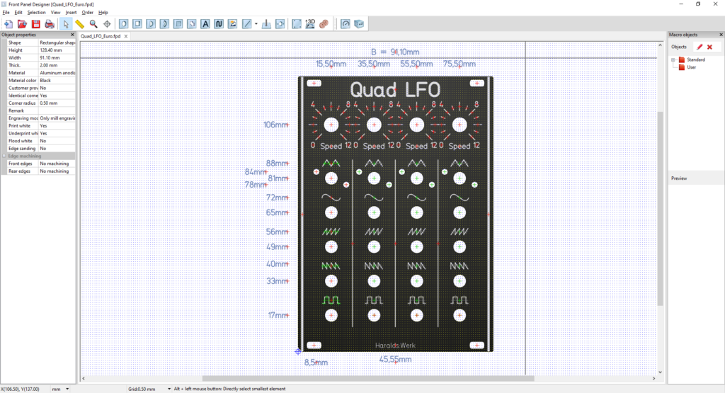
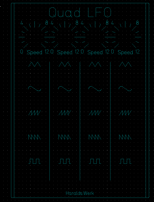
Above is a example of the Quad LFO in front panel express. On the top left side you will see the file menu. This has the option “Export” (or cntl +L)
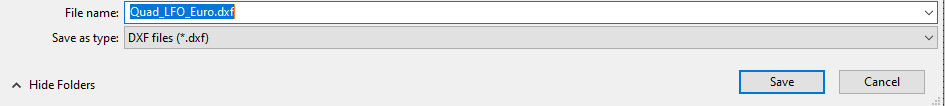
A new window will appear where you can save the file. I choose for DXF as a file type mainly because Kicad can work with DXF. When pressing save a message box will appear.
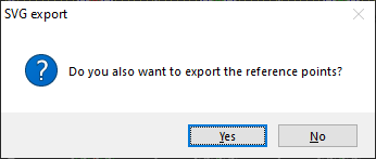
Press NO.
We now have a DXF we can use in Kicad. We start by making a new pcb with pcbnew.
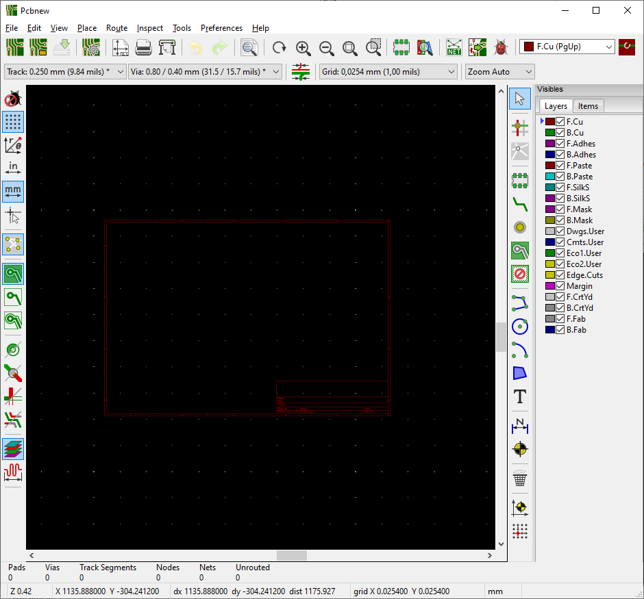
Again go to the top left and choose File. Here you have the option to “Import”. Import the graphic (DXF).
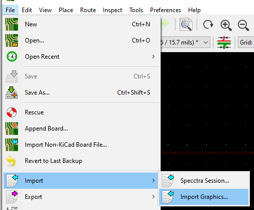
A new window will appear.
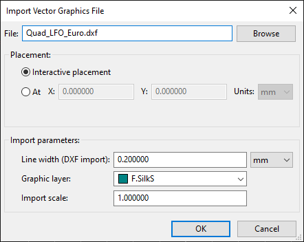
Import the graphic on the layer you want this graphic to display. I tend to use the silkscreen front and back (for lettering), the edge layer for the cut outs.
You should have something like the screenshot below
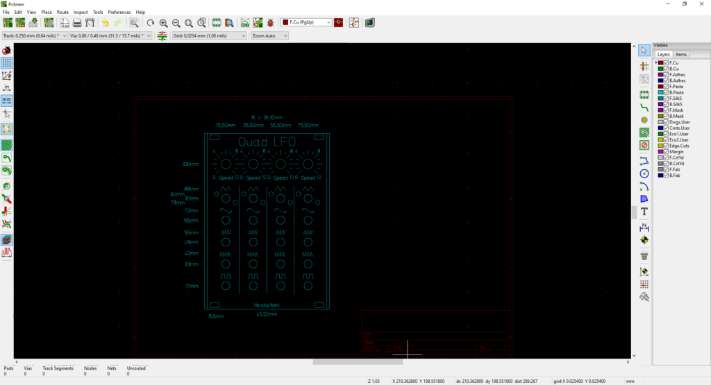
Everything is now on the silkscreen layer. I’m going to import the graphic again but this time on the edge layer and put them right on top of each other.
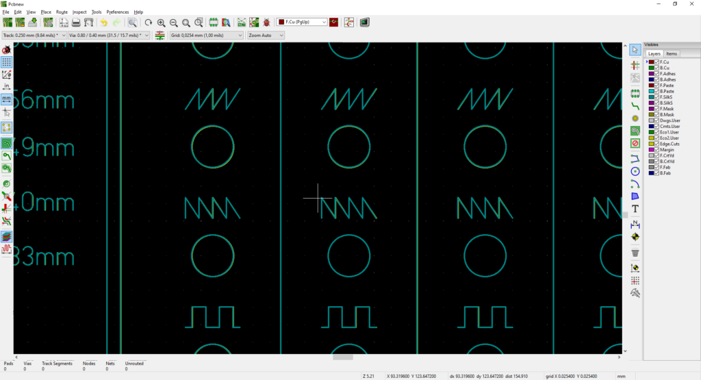
Now we can use the menu on the righthand side to turn layers on and off. And by doing so only selecting in the layers that are shown.
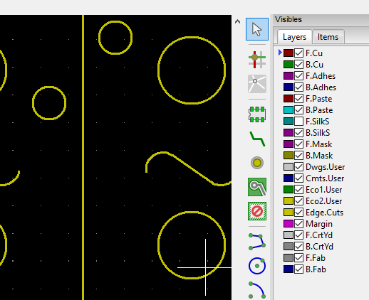
Now I start removing things just by selecting them.
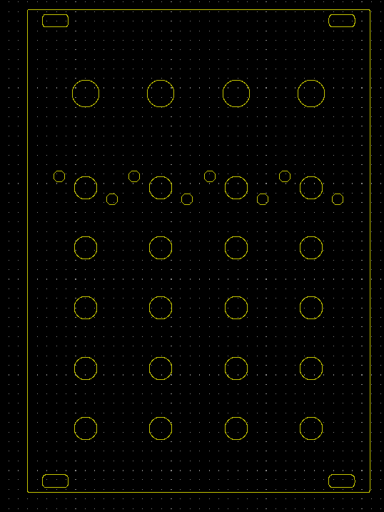
On the edge layer I only leave the holes that need to be cut.
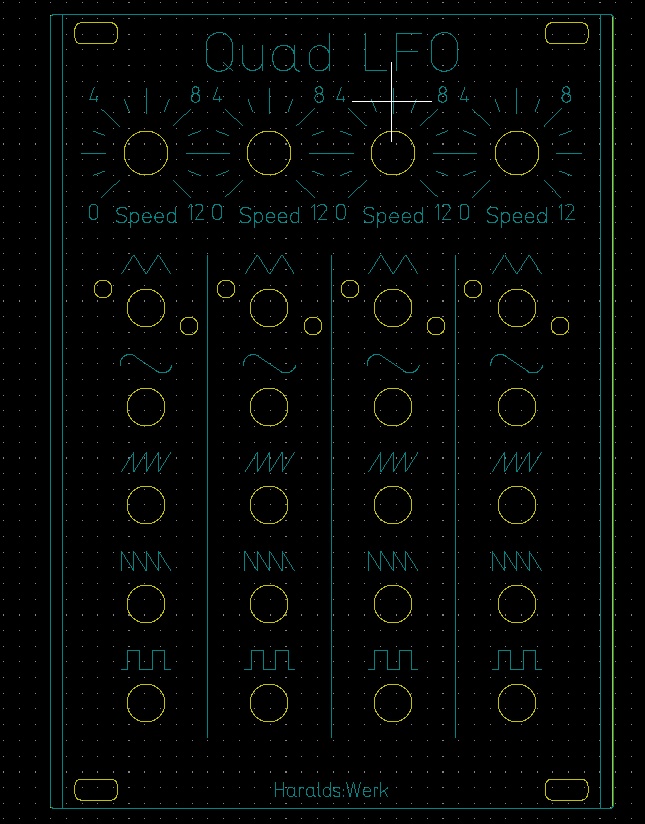
On the silkscreen I removed the holes and only leave lettering and text. When combining these two you get the result below.
From here on the panel is done, but it still can lead to questions from your manufacture. There is no copper on this board nor are there drill files. I tend to make some line on there with copper or use a filling mask. Just to avoid these questions. But from here on the main part is done. If you need a drilling file you could use the shapes for positioning your holes.
Design panels from PCB’s can be a real art. Looking at ST-modular or feedback modules, I still got a lot to learn.
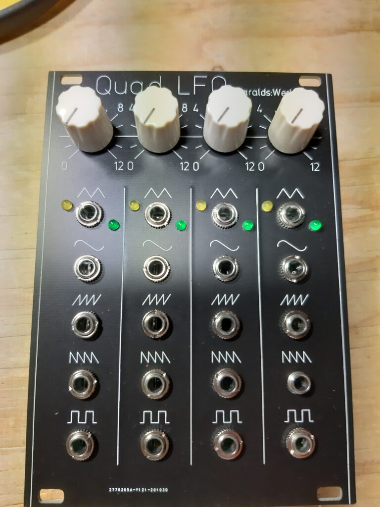
Below is the final product
I tried this with a dxf and svg I have for a veils clone called Quatro, and I got a faily decent result although not one I’d send to be fabbed just yet.
A few questions:
How did you set the panel size so it displays in JLCPCB’s order process?
When viewing in JLC, it doesn’t show any panel color changing, but I can see the silkscreen changes according to the settings, any ideas what the problem is?
How did you set the panel size so it displays in JLCPCB’s order process?
This doesn’t always work. I think JLC uses the edge cut layer for this but even the panels I made don’t display the size when uploading. Luckly for me Harlads werk come with sizes in the FPD files. Other trick would be to use the KiCad measuring tool. JLC doesn’t mind if you are a few millimeters off. Even height and width filled in the wrong way round JLC will correct this for you. But good point will going to do some research on this.
When viewing in JLC, it doesn’t show any panel color changing, but I can see the silkscreen changes according to the settings, any ideas what the problem is?
Do you mean in the Gerber preview at JLC? Normally this would change color’s when selecting it from the dropdownbox. If only the the silkscreen changes that would be a strange result. JLC preview is not the best previewer. I had some strange letttering in the preview but came out great on the pcb’s. Can you send me the Gerbers and will have a check for you.
I didn’t save the gerbers in their most final form, I was just getting a feel for how to do it, I’ve been toying with a few things over the last few days but I really should knuckle down and follow a tutorial instead of your fiddling about with snippets of info and buckets of guesswork! Thanks for your input anyway, I have your moog filter panel on the workbench right now, along with harolds PCBs at the moment, just figuring out what components I’m missing.
He let me know if the panel fit’s, I have tested it yet. It should fit ,all others do but love to see one build. Will dive into the sizing error at JLCPCB. Had that error again myself with the db ladder filter panel yesterday.
hey! the panel fit perfectly! I just found this thread and realised I never replied…
Thank you for the tricks – very well explained. Am going to download Kicad and get learning.
If any questions do come up please do ask. Will make a new post about ground/net planes. It’s not in this one but for extra thickness and sturdiness you can add planes. Copper filling the remaining board. Also less questions from JLC 🙂
Could you tell a bit more about this?
Hi Rien,
I hope this answer that question
https://www.quinie.nl/kicad-fr4-panels-using-planes-copper-areas/
Thank you