
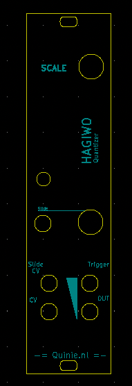
This will be a small post about using ground planes for panels made with Kicad. When making panels and sending them to the fabrications there isn’t that much need for traces. There aren’t any components on the panel just a rectangle with some holes in it.
The fabrication might ask you what to do with the copper layers when ordering them as FR4 panels. Cause it’s kinda strange making a “pcb” withut any copper lines/ traces.
In kicad there is a option to pore copper in a rectangle normally used for ground planes (or other net). When using this with panels the copper remains and your panel will be slightly thicker and more sturdy.

In Kicad 6 look for the button shown. With it you can fill an area.
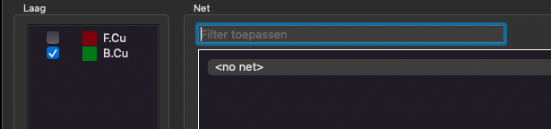
You can then select the front and back layer to fill with a net. This option I use on some modules to fill the pcb’s with ground planes. But for panels there is no net just use it to fill the copper over the whole panel.
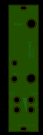
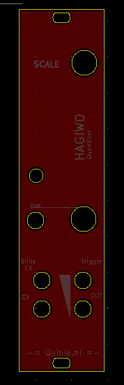
With planes on both side you will get a sturdy FR4 panel. If you are going for the aluminum option ignore the back side (send it as note to fabrication) cause aluminum only has copper on one side.
There are some videos on youtube how to work with planes.
The couple of boards I’ve made, I’ve been connecting the jacks and mounting holes to the pour and the ground net. I don’t know if this actually does anything desirable, but it does mean I can get away with not connecting all the jacks’ ground pins on passive modules.